
DS89C386
Twelve Channel CMOS Differential Line Receiver
General Description
The DS89C386 is a high speed twelve channel CMOS differ-
ential receiver that meets the requirements of TIA/
EIA-422-B. The DS89C386 features low power dissipation of
240 mW typical.
Each TRI-STATE
Æ
enable, EN, allows the receiver output to
be active or in a Hi-impedance off state. Each enable is com-
mon to only two receivers for flexibility and multiplexing of re-
ceiver outputs.
The receiver output (RO) is guaranteed to be High when the
inputs are left open and unterminated. The receiver can de-
tect signals as low and including
±
200 mV over the common
mode range of
±
7V. The receiver outputs (RO) are compat-
ible with both TTL and CMOS levels.
Features
n
Low power design -- 240 mW typical
n
Meets TIA/EIA-422-B (RS-422)
n
Receiver OPEN input failsafe feature
n
Guaranteed AC parameters:
-- Maximum receiver skew -4 ns
-- Maximum transition time -9 ns
n
High Output Drive Capability:
±
6 mA
n
Available in SSOP packaging:
-- Requires 30% less PCB space than 3 DS34C86TMs
Connection Diagram
Function Diagram
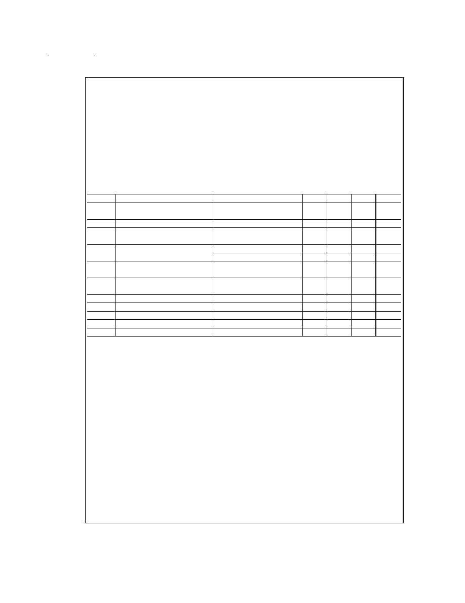
Truth Table
Enable
Inputs
Output
EN
RI≠RI
*
RO
L
X
Z
H
200 mV or OPEN
H
H
-200 mV
L
H
+200 mV
>
and
>
-200 mV
X
Not terminated.
TRI-STATE
Æ
is a registered trademark of National Semiconductor Corporation.
48L SSOP
DS89C386
DS012085-1
Order Number DS89C386TMEA
See NS Package Number MS48A
DS012085-2
1/6 of package
May 1995
DS89C386
T
welve
Channel
CMOS
Differential
Line
Receiver
© 1998 National Semiconductor Corporation
DS012085
www.national.com
Absolute Maximum Ratings
(Notes 1, 2)
If Military/Aerospace specified devices are required,
please contact the National Semiconductor Sales Office/
Distributors for availability and specifications.
Supply Voltage (V
CC
)
-0.5 to 7V
Input Common Mode Range (V
CM
)
±
14V
Differential Input Voltage (V
DIFF
)
±
14V
Enable Input Voltage (V
IN)
7V
Storage Temperature Range (T
STG
)
-65∞C to +150∞C
Lead Temperature (Soldering 4 sec)
260∞C
Maximum Power Dissipation at 25∞C (Note 4)
SSOP Package
1359 mW
Current Per Output
±
25 mA
This device does not meet 2000V ESD rating. (Note 5)
Operating Conditions
Min
Max
Unit
Supply Voltage (V
CC
)
4.50
5.50
V
Operating Temperature Range (T
A
)
DS89C386T
-40
+85
∞C
Enable Input Rise or Fall Times
500
ns
DC Electrical Characteristics
(Note 3)
V
CC
= 5V
±
10% (unless otherwise specified)
Symbol
Parameter
Conditions
Min
Typ
Max
Units
V
TH
Differential Input Voltage
V
OUT
= V
OH
or V
OL
-200
±
35
+200
mV
-7V
<
V
CM
<
+7V
V
HYST
Input Hysteresis
V
CM
= 0V
70
mV
R
IN
Input Resistance
V
IN
= -7V, +7V
5.0
6.8
10
k
(Other Input = GND)
I
IN
Input Current
V
IN
= +10V, Other Input = GND
+1.1
+1.5
mA
(Under Test)
V
IN
= -10V, Other Input = GND
-2.0
-2.5
mA
V
OH
High Level Output Voltage
V
CC
= Min., V
(DIFF)
= +1V
3.8
4.2
V
I
OUT
= -6.0 mA
V
OL
Low Level Output Voltage
V
CC
= Max., V
(DIFF)
= -1V
0.2
0.3
V
I
OUT
= 6.0 mA
V
IH
Enable High Input Level Voltage
2.0
V
CC
V
V
IL
Enable Low Input Level Voltage
GND
0.8
V
I
OZ
TRI-STATE Output Leakage Current
V
OUT
= V
CC
or GND, EN = V
IL
±
0.5
±
5.0
µA
I
I
Enable Input Current
V
IN
= V
CC
or GND
±
1.0
µA
I
CC
Quiescent Power Supply Current
V
CC
= Max., V
(DIFF)
= +1V
48
69
mA
www.national.com
2

AC Electrical Characteristics
(Note 3)
V
CC
= 5V
±
10% (
Figures 1, 2, 3)
Symbol
Parameter
Conditions
Min
Typ
Max
Units
t
PLH
,
Propagation Delay
C
L
= 50 pF
t
PHL
Input to Output
V
DIFF
= 2.5V
10
19
30
ns
V
CM
= 0V
t
SK
Skew
C
L
= 50 pF
V
DIFF
= 2.5V
0
2
4
ns
V
CM
= 0V
t
RISE
,
Output Rise and
C
L
= 50 pF
t
FALL
Fall Times
V
DIFF
= 2.5V
4
9
ns
V
CM
= 0V
t
PLZ
,
Propagation Delay
C
L
= 50 pF
t
PHZ
ENABLE to Output
R
L
= 1000
13
18
ns
V
DIFF
= 2.5V
t
PZL
,
Propagation Delay
C
L
= 50 pF
t
PZH
ENABLE to Output
R
L
= 1000
13
21
ns
V
DIFF
= 2.5V
Note 1: Absolute Maximum Ratings are those values beyond which the safety of the device cannot be guaranteed. They are not meant to imply that the device
should be operated at these limits. The table of "Electrical Characteristics" provides conditions for actual device operation.
Note 2: Unless otherwise specified, all voltages are referenced to ground.
Note 3: Unless otherwise specified, Min/Max limits apply across the operating temperature range. All typicals are given for V
CC
= 5V and T
A
= 25∞C.
Note 4: Ratings apply to ambient temperature at 25∞C. Above this temperature derate SSOP (MEA) Package 10.9 mW/∞C.
Note 5: ESD Rating: HEM (1.5 k
, 100 pF)
Inputs
2000V
Outputs
1000V
EIAJ (0
, 200 pF)
All Pins
350V
www.national.com
3

Logic Diagram
Parameter Measurement Information
DS012085-3
DS012085-4
FIGURE 1. Propagation Delays
www.national.com
4
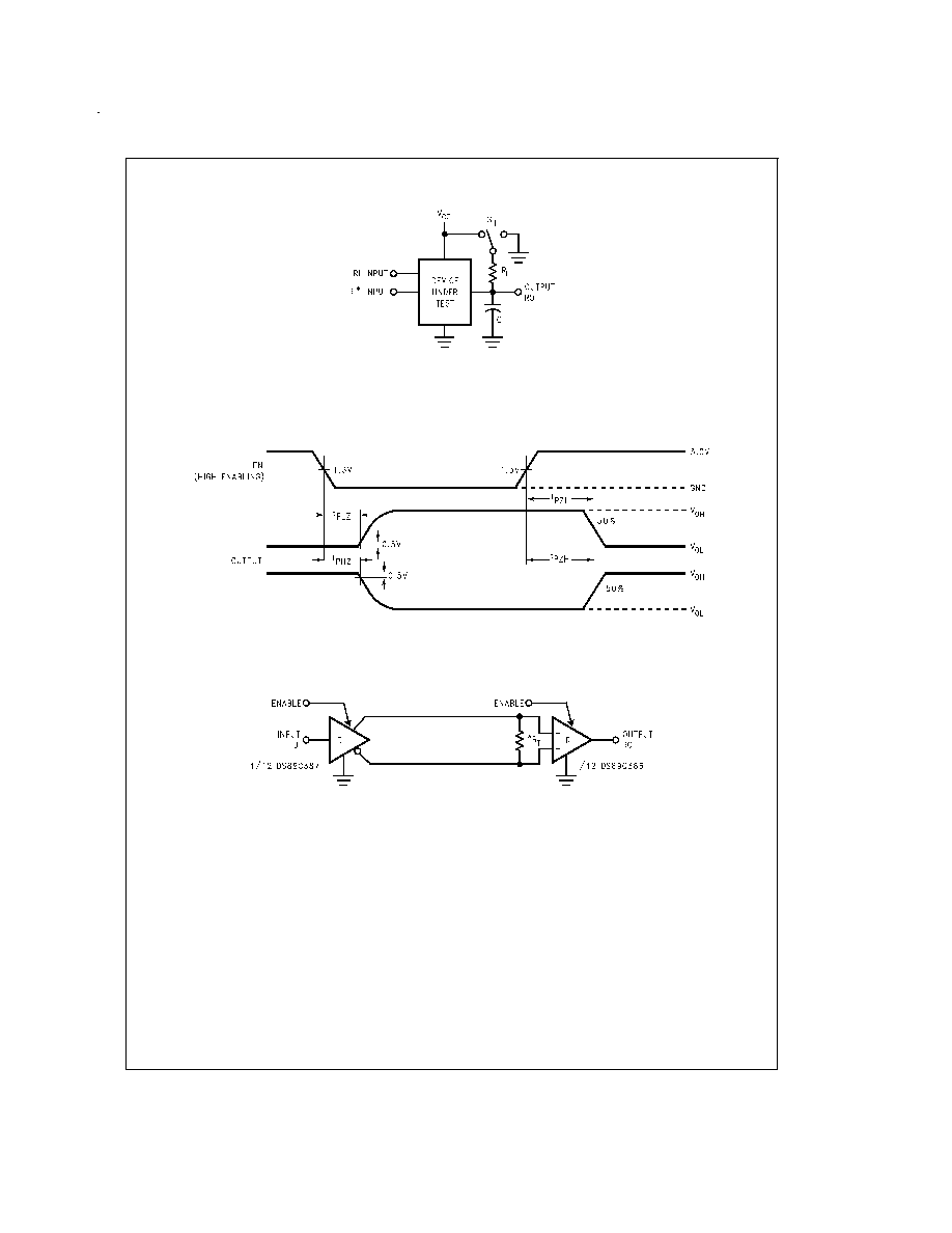
Parameter Measurement Information
(Continued)
Application Information
SKEW
Skew may be thought of in a lot of different ways, the next
few paragraphs should clarify what is represented by t
SK
in
this datasheet and how it is determined. Skew, as used in
this databook, is the absolute value of a mathematical differ-
ence between two propagation delays. This is commonly ac-
cepted throughout the semiconductor industry. However,
there is no standardized method of measuring propagation
delay, from which skew is calculated, of differential line re-
ceivers. Elucidating, the voltage level, at which propagation
delays are measured, on both input and output waveforms
are not always consistant. Therefore, skew calculated in this
datasheet, may not be calculated the same as skew defined
in another. This is important to remember whenever making
a skew comparison.
Skew may be calculated for the DS89C386, from many dif-
ferent propagation delay measurements. They may be clas-
sified into two categories, single-ended and differential.
Single-ended skew is calculated from t
PHL
and t
PLH
propaga-
tion delay measurements (see
Figures 5, 6). Differential
skew is calculated from t
PHLD
and t
PLHD
differential propaga-
tion delay measurements (see
Figures 7, 8).
DS012085-5
C
L
Includes load and test jig capacitance.
S1 = V
CC
for t
PZL
, and t
PLZ
measurements.
S1 = GND for t
PZH
, and t
PHZ
measurements.
S1 = Open for t
PLH
, t
PHL
, and t
SK
.
FIGURE 2. Test Circuit for Switching Characteristics
DS012085-6
FIGURE 3. TRI-STATE Output Enable and Disable Waveforms
DS012085-7
* R
T
is optional although highly recommended to reduce reflections.
FIGURE 4. Two-Wire Balanced System, RS-422
www.national.com
5